PN junction depletion modulator#
# !uv add femwell  # uncomment to install
#! uvx inc run gmsh
/home/runner/work/simulation-templates/simulation-templates/.venv/lib/python3.12/site-packages/femwell/pn_analytical.py:8: SyntaxWarning: invalid escape sequence '\m'
  (3) M. Nedeljkovic, R. Soref and G. Z. Mashanovich, "Free-Carrier Electrorefraction and Electroabsorption Modulation Predictions for Silicon Over the 1–14- $\mu\hbox{m}$ Infrared Wavelength Range," in IEEE Photonics Journal, vol. 3, no. 6, pp. 1171-1180, Dec. 2011, doi: 10.1109/JPHOT.2011.2171930.
We can study the propagation constant in waveguides as a function of arbitrary physics. Here, we consider the depletion approximation to pn junctions to study how doping level and junction placement affect modulation in a doped silicon waveguide. This is a simple, yet common, approximation [1].
clad_thickness = 2
slab_width = 3
wg_width = 0.5
wg_thickness = 0.22
slab_thickness = 0.09
core = shapely.geometry.box(
-wg_width / 2, -wg_thickness / 2, wg_width / 2, wg_thickness / 2
)
slab = shapely.geometry.box(
-slab_width / 2,
-wg_thickness / 2,
slab_width / 2,
-wg_thickness / 2 + slab_thickness,
)
clad = shapely.geometry.box(
-slab_width / 2, -clad_thickness / 2, slab_width / 2, clad_thickness / 2
)
polygons = OrderedDict(
core=core,
slab=slab,
clad=clad,
)
resolutions = dict(
core={"resolution": 0.02, "distance": 0.5},
slab={"resolution": 0.04, "distance": 0.5},
)
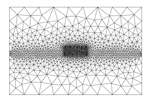
mesh = from_meshio(
mesh_from_OrderedDict(polygons, resolutions, default_resolution_max=10)
)
mesh.draw().show()
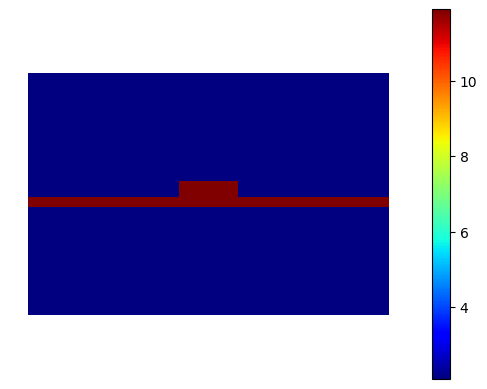
To define the epsilon, we proceed as for a regular waveguide, but we superimpose a voltage-dependent index of refraction based on the Soref Equations [2], [3]. These phenomenologically relate the change in complex index of refraction of silicon as a function of the concentration of free carriers. We model the spatial distribution of carriers according to the physics of a 1D PN junction in the depletion approximation. For more accurate results, full modeling of the silicon processing and physics through TCAD must be performed.
xpn = 0
NA = 1e18
ND = 1e18
V = 0
wavelength = 1.55


def define_index(mesh, V, xpn, NA, ND, wavelength):
    basis0 = Basis(mesh, ElementTriP0())
    epsilon = basis0.zeros(dtype=complex)
    for subdomain, n in {"core": 3.45, "slab": 3.45}.items():
        epsilon[basis0.get_dofs(elements=subdomain)] = n
    epsilon += basis0.project(
        lambda x: index_pn_junction(x[0], xpn, NA, ND, V, wavelength),
        dtype=complex,
    )
    for subdomain, n in {"clad": 1.444}.items():
        epsilon[basis0.get_dofs(elements=subdomain)] = n
    epsilon *= epsilon  # square now
    return basis0, epsilon


basis0, epsilon = define_index(mesh, V, xpn, NA, ND, wavelength)
basis0.plot(epsilon.real, colorbar=True).show()
basis0.plot(epsilon.imag, colorbar=True).show()
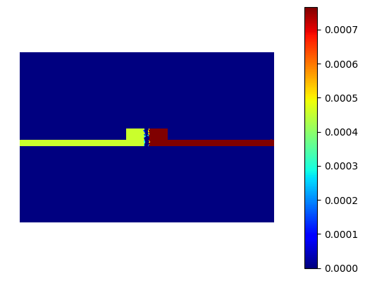
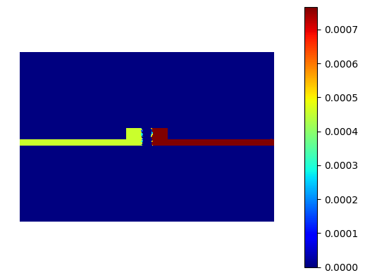
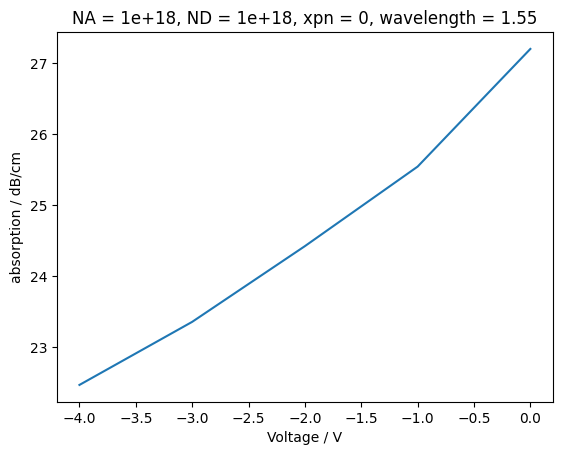
The index change is weak compared to the contrast between silicon and silicon dioxide, but it is accompanied by a change in absorption which is easier to observe. As voltage is increased, the region without charge widens, which is the mechanism behind depletion modulation:
V = -4
basis0, epsilon = define_index(mesh, V, xpn, NA, ND, wavelength)
basis0.plot(epsilon.imag, colorbar=True).show()
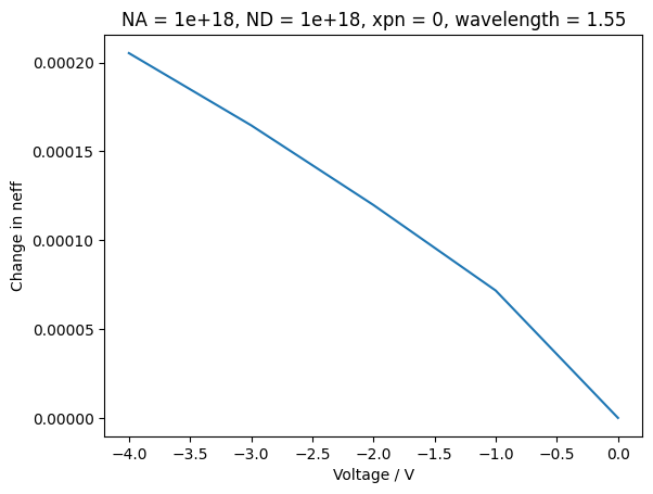
And now we can mode solve as before, and observe the change in effective index and absorption of the fundamental mode as a function of applied voltage for given junction position and doping levels:
voltages = [0, -1, -2, -3, -4]
neff_vs_V = []
for V in voltages:
    basis0, epsilon = define_index(mesh, V, xpn, NA, ND, wavelength)
    modes = compute_modes(basis0, epsilon, wavelength=wavelength, num_modes=1, order=2)
    neff_vs_V.append(modes[0].n_eff)
Integrating electric field components over the cross-section#
The mode solver returns an electric field E composed of transverse and longitudinal parts.
When interpolated onto the mesh via basis.interpolate(E), the result has two entries:
E[0]: a 2-component vector containing the transverse field components(Ex, Ey)E[0][0]→ ExE[0][1]→ Ey
E[1]: a scalar containing the longitudinal componentEz
To integrate a quantity like |Ex|² over the waveguide cross-section, we use scikit-fem’s
@Functional decorator. A Functional defines an integrand evaluated at every quadrature
point; calling .assemble() performs the numerical integration over the mesh.
The calculate_confinement_factor method in femwell uses the same pattern — the expression
dot(conj(w["E"][0]), w["E"][0]) computes |Ex|² + |Ey|² (transverse intensity), and
conj(w["E"][1]) * w["E"][1] computes |Ez|².
from skfem import Functional
from skfem.helpers import dot

# Compute one mode at V = 0 for the integration demo
basis0, epsilon = define_index(mesh, V=0, xpn=xpn, NA=NA, ND=ND, wavelength=wavelength)
modes = compute_modes(basis0, epsilon, wavelength=wavelength, num_modes=1, order=2)
mode = modes[0]


# --- Integrate |Ex|^2 over the full cross-section ---
@Functional(dtype=complex)
def Ex_squared(w):
    return np.conj(w["E"][0][0]) * w["E"][0][0]  # |Ex|^2


int_Ex2 = np.real(Ex_squared.assemble(mode.basis, E=mode.basis.interpolate(mode.E)))
print(f"|Ex|^2 integrated over full cross-section: {int_Ex2:.6e}")


# --- Integrate |Ey|^2 ---
@Functional(dtype=complex)
def Ey_squared(w):
    return np.conj(w["E"][0][1]) * w["E"][0][1]  # |Ey|^2


int_Ey2 = np.real(Ey_squared.assemble(mode.basis, E=mode.basis.interpolate(mode.E)))
print(f"|Ey|^2 integrated over full cross-section: {int_Ey2:.6e}")


# --- Integrate |Ex|^2 + |Ey|^2 (total transverse intensity) ---
@Functional(dtype=complex)
def E_transverse_squared(w):
    return dot(np.conj(w["E"][0]), w["E"][0])  # |Ex|^2 + |Ey|^2


int_Et2 = np.real(
    E_transverse_squared.assemble(mode.basis, E=mode.basis.interpolate(mode.E))
)
print(f"|Ex|^2 + |Ey|^2 integrated over full cross-section: {int_Et2:.6e}")
print(f"TE fraction (Ex / transverse): {int_Ex2 / int_Et2:.4f}")
|Ex|^2 integrated over full cross-section: 1.361880e+02
|Ey|^2 integrated over full cross-section: 1.918958e+00
|Ex|^2 + |Ey|^2 integrated over full cross-section: 1.381070e+02
TE fraction (Ex / transverse): 0.9861
# --- Restrict integration to the core region only ---
core_basis = mode.basis.with_elements("core")

int_Ex2_core = np.real(
    Ex_squared.assemble(core_basis, E=core_basis.interpolate(mode.E))
)
int_Et2_core = np.real(
    E_transverse_squared.assemble(core_basis, E=core_basis.interpolate(mode.E))
)
print(f"|Ex|^2 integrated over core only: {int_Ex2_core:.6e}")
print(f"|Ex|^2 + |Ey|^2 integrated over core only: {int_Et2_core:.6e}")
print(f"Confinement (transverse E in core / total): {int_Et2_core / int_Et2:.4f}")
|Ex|^2 integrated over core only: 8.762818e+01
|Ex|^2 + |Ey|^2 integrated over core only: 8.825605e+01
Confinement (transverse E in core / total): 0.6390
Bibliography#
Lukas Chrostowski and Michael Hochberg. Silicon Photonics Design: From Devices to Systems. Cambridge University Press, Cambridge, England, UK, March 2015. ISBN 978-1-10708545-9. URL: https://doi.org/10.1017/CBO9781316084168, doi:10.1017/CBO9781316084168.
R. Soref and B. Bennett. Electrooptical effects in silicon. IEEE J. Quantum Electron., 23(1):123–129, January 1987. URL: https://doi.org/10.1109/JQE.1987.1073206, doi:10.1109/JQE.1987.1073206.
Milos Nedeljkovic, Richard Soref, and Goran Z. Mashanovich. Free-Carrier Electrorefraction and Electroabsorption Modulation Predictions for Silicon Over the 1–14- µm Infrared Wavelength Range. IEEE Photonics J., 3(6):1171–1180, October 2011. URL: https://doi.org/10.1109/JPHOT.2011.2171930, doi:10.1109/JPHOT.2011.2171930.